

A team of researchers led by City University of Hong Kong (CityU) has achieved a significant breakthrough in the synthesis of high-quality, semiconducting nanomesh. This groundbreaking method offers lower production costs and operates at a lower temperature compared to traditional techniques. The team’s findings have the potential to revolutionize the large-scale production of nanomesh, opening doors for next-generation electronics.
Nanomesh is a nano-scale material composed of a network of nanowires. Over the past few decades, nanowires made of crystalline inorganic materials have been extensively explored for their potential in emerging electronics. These nanowires possess remarkable features such as mechanical flexibility, energy efficiency, and optical transparency. However, the scalability, integrability, and cost-effectiveness of nanowire semiconductors have been limiting factors, restricting their application in large-area electronic and optoelectronic domains.
To address these limitations, a team of scientists from CityU has developed a breakthrough vapor-phase growth method that operates at lower temperatures. This method allows for the large-scale synthesis of semiconducting tellurium (Te) nanomesh, which holds great promise for meeting the technological demands of today’s Internet of Things (IoT) applications.
Professor Johnny Ho Chung-yin, Associate Head and Professor in the Department of Materials Science and Engineering (MSE) at CityU, expressed his optimism about the use of tellurium nanomesh in electronics. He stated, “The progress made in this research marks a significant step towards the large-scale production of functional “tellurium nanomesh”, enabling potential applications that are not achievable through other means.”
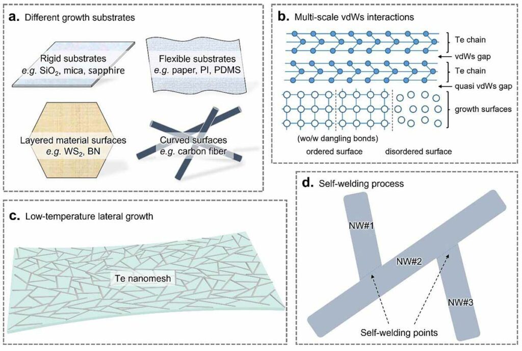
The newly developed method enables the production of high-quality tellurium nanomesh on various substrates, including silicon oxide, polymers (stretchable plastics), and even paper. It offers scalability and cost-effectiveness, as demonstrated by the research team’s publication in the journal Nature Communications, titled “Van der Waals nanomesh electronics on arbitrary surfaces.”
The growth process begins by vaporizing tellurium source powders, which are then transported to growth substrates and heated at 100°C with a flow of argon gas. Through the application of the principle of multi-scale van der Waals interactions, the research team successfully created nanomeshes comprising self-assembled and self-welding tellurium nanowires. These nanowires are laterally vapor-grown on various surfaces at the low temperature of 100°C, a feat that was previously impossible using conventional methods.
The use of a lower temperature in the synthesis process and the ability to grow nanomesh on diverse substrates contribute to lower production costs. Additionally, the discovery of a self-welding process during the growth of tellurium nanomesh enhances device performance and ensures the mechanical robustness of flexible electronics.
The team’s experiments showcased the multi-functional applications of tellurium nanomesh, including micrometer-level patterning, the fabrication of high-mobility transistors, and the production of fast and sensitive infrared photodetectors with a photoresponse time under 3 microseconds, all achieved on paper.
Professor Ho emphasized the promising nature of these achievements, stating, “All the obtained device metrics are on par with state-of-the-art devices but can be produced at a lower cost. They are promising for meeting emerging technological demands.” He further explained that this latest development enhances the transport and photoelectric properties of nanomesh and resolves concerns regarding compatibility between the target device substrate and the nanomesh growth process. As a result, devices can now be produced on a wide range of technologically functional surfaces in a scalable and cost-effective manner.
FAQ
Nanomesh is a nano-scale material formed from a network of nanowires.
Nanowire semiconductors have limitations in terms of scalability, integrability, and cost-effectiveness, which restrict their application in large-area electronic and optoelectronic domains.
The discovery of the cost-effective method for large-scale nanomesh production opens doors for next-generation electronics and enables the realization of potential applications that were previously unachievable.
Tellurium nanomesh holds great promise for meeting the technological demands of today’s Internet of Things (IoT) applications due to its unique properties. It can enhance the performance of devices and facilitate their production on a wide range of technologically functional surfaces.
Growing nanomesh on diverse substrates, such as silicon oxide, polymers, and even paper, allows for scalability, cost-effectiveness, and compatibility with a wide range of technologically functional surfaces.
More information: Nature Communications (2023). DOI: 10.1038/s41467-023-38090-8